

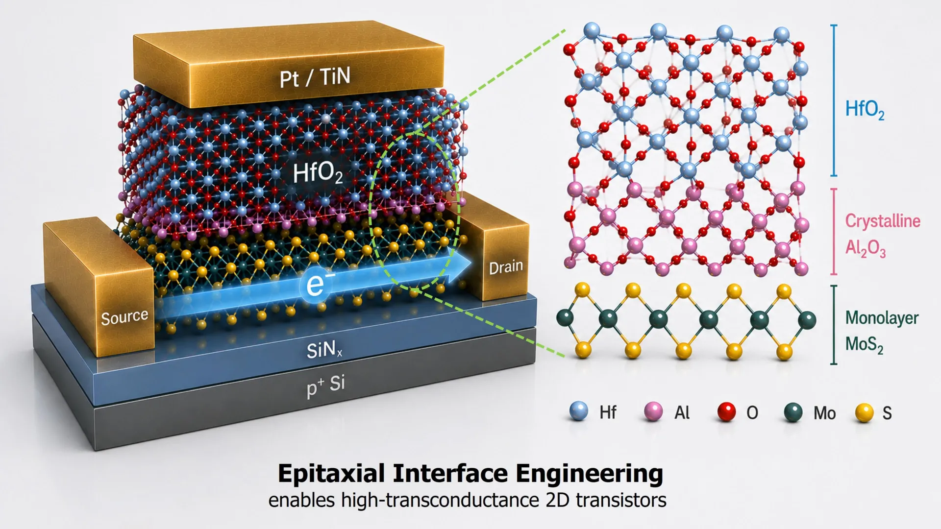
Scientists at National Yang Ming Chiao Tung University and TSMC Corporate Research have developed a new approach to a longstanding challenge in two-dimensional semiconductor technology. Their work, published in Nature Electronics, addresses a fundamental trade-off that has limited the performance of transistors built from atomically thin materials.
The core problem has centered on the gate dielectric, an insulating layer critical to transistor operation. As devices shrink, thinner dielectric layers improve electrical control, but adding these layers to atomically thin semiconductors typically damages the interface between materials, reducing electron mobility and negating performance gains. Engineers have faced a difficult choice between stronger control and better charge carrier movement.
Rather than searching for new semiconductor materials or dielectric compounds, the research team focused on the boundary region itself. They developed a method using an ultrathin epitaxial aluminum layer deposited directly onto molybdenum disulfide, which was then oxidized to create an aluminum oxide buffer approximately 0.42 nanometers thick. A hafnium oxide gate dielectric was subsequently added atop this engineered interface. This buffer layer serves dual functions: it allows the hafnium oxide to grow uniformly across the semiconductor surface and protects electrons from unwanted electrical interactions at the material boundary.
Testing of devices fabricated using this approach demonstrated significant improvements. The transistors achieved an equivalent oxide thickness of roughly one nanometer while maintaining low leakage current, minimal hysteresis, and strong electrostatic control. Importantly, they sustained efficient carrier transport, marking the first demonstration of combining all three capabilities simultaneously in atomically thin transistors. The researchers used chemically vapor-deposited materials rather than mechanically exfoliated samples, bringing the technology closer to scalable manufacturing processes.
The findings suggest a broader shift in semiconductor design philosophy. As transistor dimensions approach atomic scales, the interfaces between materials may become as important as the materials themselves. Researchers increasingly recognize that these atomic-scale boundaries, though only a few atoms thick, can significantly influence device performance and that engineering these interfaces with precision may be essential for advancing semiconductor technology beyond traditional silicon scaling.
Article Attribution | Read More at Article Source
Article summary produced by Claude AI